
PCB Design & Layout Services
Bernini Design SRL provides professional PCB layout services for complex electronic applications. We combine over 40 years of hardware design experience with the industry-standard Altium Designer platform to deliver robust, high-performance circuit boards.
Our Engineering Focus
We specialize in high-density, multi-layer designs, including:
Wireless Integration: Specialized routing for Bluetooth and GSM/LTE modules.
Complex Multi-layer Architectures: Precision trace routing for signal integrity and thermal management.
Flexible Support: Custom board shapes and component placement optimization tailored to your mechanical constraints.
Design for Manufacturing (DFM): Solutions engineered for cost-effectiveness and high-yield production to optimize your return on investment.
Request a Quote
To receive a technical assessment and a formal quotation, please forward your schematic diagrams and Bill of Materials (BOM) to: bernini@bernini-design.com
Technical FAQ
How are design costs calculated? Pricing is determined by board complexity, layer count, signal speed requirements, and required turnaround time.
Can you provide manufacturing files? Yes, we deliver full Gerber files, BOMs, and assembly drawings ready for immediate fabrication.
What software do you use? We utilize the Altium platform to ensure industry-standard compliance and seamless integration with manufacturing partners.
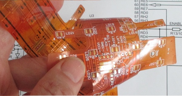
PCB LAYOUT DESIGN SERVICES PRICE LIST
At Bernini Design SRL, we like to focus on designing PCB layouts because we like difficult things. Despite the fact that PCB layout designing is an intricate process, our team has the specialized skills required to provide the best solution. At Bernini Design SRL, the PCB layouts are designed with superior technology thanks to our team of skilled engineers. Bernini Design SRL is a top electronic industry expert using the cutting-edge ALTIUM platform. We specialize in designing Bluetooth modules, GSM equipment, and multi-layered PCB layouts based on flexible support. We design cost-effective solutions as well. This will allow you to optimize your ROI.
GET A QUOTE NOW MAIL TO SUPPORT@BERNINI-DESIGN.COM
How much does it cost to print a circuit board?
How much does a PCB board cost?
How do I print a PCB board?
THIS PAGE PROVIDE ANSWERS TO FAQ ABOUT PRINTED CIRCUIT BOARD PRICE
EXAMPLES OF THE PRICE OF OUR PCB LAYOUT DESIGN SERVICES
DESCRIPTION: gold-plated printed circuit board suitable for industrial power supply application. The board contains mixed PTH and SMT components. The board features mechanical milling to protect against high-voltage surges.

SINGLE PCB DIMENSIONS: 125mmX140mmX1.57mnn (4.9" X 5,5" X 0.063 ")
PCB (PANEL) DIMENSIONS: the same as above
MATERIAL: FR4
NOTES: GOLD PLATED
LAYOUT DESIGN PRICE: 240€
TOOLING COST (ONE TIME): 125€
SAMPLES: 3 PCS FREE OF CHARGE
PCB PRICE (10-20PCS): 5.5€
PCB PRICE (250-500PCS): 3,8€
DESCRIPTION: printed circuit board suitable for industrial power supply application. The board contains mixed PTH and SMT components. The board features mechanical milling and several holes to allow installing power switches.
SINGLE PCB DIMENSIONS: 90mmX90mmX1.57mnn (3.54" X 3,54" X 0.062 ")
PCB (PANEL) DIMENSIONS: 190mmX190mm (7.48" X 7,48")
MATERIAL: FR4 35um Copper
NOTES: LF-HAL
LAYOUT DESIGN PRICE: 145€
TOOLING COST (ONE TIME): 118€
SAMPLES: 3 PCS FREE OF CHARGE
PCB PRICE (10-20PCS): 1,4€
PCB PRICE (250-500PCS): 0,7€
DESCRIPTION: printed circuit board suitable for industrial I/O controller. The board contains mixed PTH and SMT components. The board features 70um copper thickness allowing high current surge.
SINGLE PCB DIMENSIONS: 80mmX180mmX1.57mnn (3.14" X 7,08" X 0.062 ")
PCB (PANEL) DIMENSIONS: as above, same dimensions
MATERIAL: FR4 70um Copper
NOTES: LF-HAL
LAYOUT DESIGN PRICE: 139€
TOOLING COST (ONE TIME): 120€
SAMPLES: 3 PCS FREE OF CHARGE
PCB PRICE (10-20PCS): 1,9€
PCB PRICE (250-500PCS): 1,3€
DESCRIPTION: printed circuit board suitable for measurement equipment. The board contains mixed PTH and SMT components. The board features mechanical milling to protect against high-voltage surges and to facilitate panel disassembly.

SINGLE PCB DIMENSIONS: 80mmX40mmX1.57mnn (3.14" X 1,57" X 0.063 ")
PCB (PANEL) DIMENSIONS: 160mmX90mm (6.3" X 3,54")
MATERIAL: FR4 35um Copper
NOTES: LF-HAL
LAYOUT DESIGN PRICE: 160€
TOOLING COST (ONE TIME): 120€
SAMPLES: 3 PCS FREE OF CHARGE
PCB PRICE (10-20PCS): 0,9€
PCB PRICE (250-500PCS): 0,48€
Ready for manufacturing? Happy to serve you with our
Electronic Manufacturing Serices
Message us on WhatsApp – We're here 24/7/36

+40 721 241 36
BERNINI DESIGN SRL
Via San Romano Casetto 26A
46035 Ostiglia (Italy)
bernini@bernini-design.com
+39 335 70 77 148